
Privacy statement: Your privacy is very important to Us. Our company promises not to disclose your personal information to any external company with out your explicit permission.
Ultra-precision machining is a necessary means of achieving high shape accuracy, surface accuracy and surface integrity. Advanced ceramic or optical glass components used in precision optics, mechanical, and electronic systems typically require very high shape accuracy and surface accuracy (eg, 0.1 nm surface roughness) and a small process metamorphic layer. Mastering the material removal rules and damage layer characteristics during ultra-precision machining is very important to improve the stability and economy of processing. The ultra-precision cutting, ultra-precision grinding and ultra-precision grinding and polishing techniques in ultra-precision machining are reviewed, and various typical processing methods and material removal mechanisms are highlighted. The above-mentioned types of ultra-precision machining methods are compared from the viewpoints of machining accuracy and machining efficiency, and a semi-fixed abrasive grain processing technique for achieving high-efficiency precision machining is introduced. Forecast the development trend of ultra-precision machining.
1. Preface
Ultra-precision machining technology is an important supporting technology for modern high-tech warfare, the basis for the development of modern high-tech industries and science and technology, and the development direction of modern manufacturing science. High-performance weapons supported by ultra-precision machining technology, processes and results for the first Gulf War (1992), the Kosovo War (1996), the Afghanistan War (1999), and the Second Gulf War (2003) Played a decisive role. The three generations of semiconductor devices supported by ultra-precision processing technology laid the foundation for the development of electronics and information industry. The development of modern science and technology is based on experiments, and almost no test equipment and equipment are required to support the ultra-precision machining technology. From macro manufacturing to micro-manufacturing is one of the future development trends of the manufacturing industry. At present, ultra-precision machining has entered the nano-scale, and nano-manufacturing is the forefront of ultra-precision machining. The developed countries of the world attach great importance to it. The recently launched research programs include the 2001 NNI (National nanotechnology initiative) program, the UK's Interdisciplinary research collaboration in nano-chnology, and the 2002 Japan Nanotechnology Support Program. The current ultra-precision machining is based on the premise of not changing the physical properties of the workpiece material to obtain ultimate shape accuracy, dimensional accuracy, surface roughness, surface integrity (no or minimal surface damage, including microcracks and other defects, residual stress). Organizational changes)
For the goal.
The research content of ultra-precision machining, that is, the factors affecting the precision of ultra-precision machining include: ultra-precision machining mechanism, processed materials, ultra-precision machining equipment, ultra-precision machining tools, ultra-precision machining fixtures, ultra-precision machining inspection and error Compensation, ultra-precision machining environment (including constant temperature, vibration isolation, clean control, etc.) and ultra-precision machining processes. All along, domestic and foreign scholars have carried out systematic research around these contents.
At the International Production Engineering Conference in 1983, TANIGUCHI described the ultra-precision machining conditions at that time and predicted the development trend of ultra-precision machining. In the following 20 years, ultra-precision machining technology has flourished. This paper reviews the current state of ultra-precision machining. Section 1 describes the development of ultra-precision machining and its driving factors. Section 2 introduces ultra-precision machining materials with a focus on advanced ceramic materials. Section 3 classifies ultra-precision machining into ultra-precision machining, ultra-precision grinding and ultra-precision grinding and polishing, and introduces typical machining techniques (generalized ultra-precision machining also includes micro-machining technology). Section 4 compares the above-mentioned types of ultra-precision machining techniques from the perspective of machining accuracy and machining efficiency, and introduces the semi-fixed abrasive processing method. Section 5 predicts the development trend of ultra-precision machining.
2. Development of ultra-precision machining
The development of ultra-precision machining has gone through the following three stages.
(1) The technology pioneering period from the 1950s to the 1980s. In the late 1950s, due to the development of cutting-edge technologies such as aerospace and defense, the United States took the lead in developing ultra-precision machining technology and developed ultra-precision cutting of diamond tools, Single Point Diamond Turning (SPDT). Also known as "micro-inch technology" for processing laser nuclear fusion mirrors, tactical missiles and manned spacecraft spherical, aspherical large parts. Since 1966, Union Carbide in the United States, Philips in the Netherlands, and Lawrence Livermore Laboratories in the United States have launched their own ultra-precision diamond lathes, but their applications are limited to experimental research by a few large companies and research units, and for defense or scientific research purposes. The main products are processed. During this period, the diamond lathe was mainly used for the processing of soft metals such as copper and aluminum, and it was also possible to process workpieces with complicated shapes, but only for axially symmetric workpieces such as aspherical mirrors.
(2) The early 1980s to the 1990s was the beginning of private industrial applications. In the 1980s, the US government promoted the commercialization of ultra-precision processing equipment by several private companies such as Moore Special Tool and Pneumo Precision, and several Japanese companies such as Toshiba and Hitachi and Cranfield University in Europe also launched products. These devices began to be manufactured for general consumer industrial optical component goods. However, the ultra-precision processing equipment at this time is still noble and rare, and is mainly ordered in the form of a dedicated machine. During this period, in addition to diamond lathes that process soft metals, ultra-precision diamond grinding that can process hard metals and hard and brittle materials has also been developed. The technology features a high-rigidity mechanism for ductile grinding of brittle materials with minimal depth of cut to achieve nanoscale surface roughness for hard metals and brittle materials. Of course, its processing efficiency and complexity of the mechanism cannot be compared to diamond lathes. In the late 1980s, the United States invested huge amounts of money and a large amount of manpower through the “Laser Nuclear Fusion Project” of the Ministry of Energy and the “Advanced Manufacturing Technology Development Plan” of the Army, Navy and Air Force. Micro-inch ultra-precision machining of large parts. The Large Optics Diamond Turning Machine (LODTM) developed by LLL National Laboratory in the United States has become a classic in the history of ultra-precision machining. This is a vertical lathe with a maximum diameter of 1.625 m and a positioning accuracy of 28 nm. With the online error compensation capability, it can be processed with a length of more than 1 m and a straightness error of only ±25 nm.
(3) The mature period of private industrial application since the 1990s. Since 1990, the demand for ultra-precision processing machines has increased dramatically due to the booming industries such as automotive, energy, medical equipment, information, optoelectronics and communications. Applications in the industry include aspherical optical lenses, Fresnel lenses, and ultra-precision molds. , disk drive heads, disk substrate processing, semiconductor wafer cutting, etc. During this period, related technologies of ultra-precision processing equipment, such as controllers, laser interferometers, air bearing precision spindles, air bearing guides, hydraulic bearing guides, and friction-driven feed shafts have gradually matured, and ultra-precision machining equipment has become Production machinery and equipment common in the industry, many companies, even small companies have also introduced mass production equipment. In addition, the accuracy of the equipment is gradually approaching the nanometer level, the processing stroke becomes larger, and the processing application is gradually widened. In addition to the diamond lathe and ultra-precision grinding, ultra-precision five-axis milling and flying cutting technology have also been developed and can be Processing of non-axisymmetric aspherical optical lenses.
At present, the world's ultra-precision processing powers are dominated by Europe, America and Japan, but the research focus of the two is not the same. Europe and the United States have paid great attention to energy or space development, especially in the United States. For decades, they have invested heavily in research on the processing of large-diameter mirrors for large-scale ultraviolet and X-ray telescopes. For example, the Space Development Program promoted by the US Space Agency (NASA) aims to produce mirrors of more than 1 m in order to detect shortwaves (0.1 to 30 nm) such as X-rays. Due to the high energy density of the X-ray, the surface roughness of the mirror must be increased to an angstrom level to increase the reflectivity. At present, the material of such a mirror is silicon carbide with good mass and good thermal conductivity, but the hardness of silicon carbide is very high, and ultra-precision grinding processing is required. Japan's research on ultra-precision machining technology started relatively late in the United States and Britain, but it is the fastest growing country in the world. Most of the applications for ultra-precision machining in Japan are civilian products, including office automation equipment, video equipment, precision measuring instruments, medical equipment and artificial organs. Japan has advantages in ultra-precision processing technology for small, ultra-small electronic and optical components in sound, light, image, and office equipment, even surpassing the United States. Japan's ultra-precision machining began with diamond cutting of aluminum and copper hubs, and then concentrated on mass production of computer hard disk magnetic sheets, followed by rapid diamond cutting of polygon mirrors for laser printers and the like, followed by optical components such as aspherical lenses. Ultra-precision cutting. An aspherical lens used in the Eastman Kodak digital camera, which was launched in 1982, has attracted widespread attention in the Japanese industry. Because an aspheric lens can replace at least three spherical lenses, the optical imaging system is compact and lightweight. Widely used in cameras, video recorders, industrial television, robot vision, CD, VCD, DVD, projectors and other optoelectronic products. Therefore, the precision forming of aspherical lenses has become a research hotspot in the Japanese optical industry.
Despite the changes of the times, the ultra-precision machining technology is constantly updated, the machining accuracy is continuously improved, and the research focus between countries is different, but the factors that promote the development of ultra-precision machining are essentially the same. These factors can be summarized as follows.
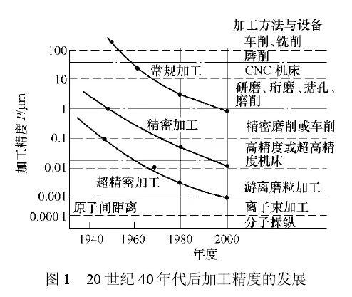
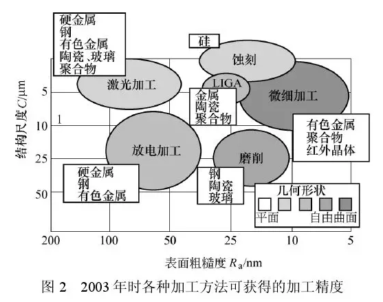
(1) The pursuit of high quality products. In order to achieve higher disk storage density or better optical performance of the lens, it is necessary to obtain a surface having a lower roughness. In order for the function of the electronic component to function properly, it is required that the processed surface does not remain in the processed layer. According to the technical requirements of the American Society for Microelectronics (SIA), the head of the next-generation computer hard disk requires a surface roughness Ra ≤ 0.2 nm, the disk requires a surface scratch depth h ≤ 1 nm, and the surface roughness Ra ≤ 0.1 nm. In 1983, TANIGUCHI summarized the processing precision of each period and predicted its development trend. Based on this, BYRNE et al. described the development of processing precision in the 1940s, as shown in Figure 1. Figure 2 shows the machining accuracy available for various machining methods in 2003. Among them, microfabrication can realize processing with a feature size of 1 μm and a surface roughness of 5 nm.
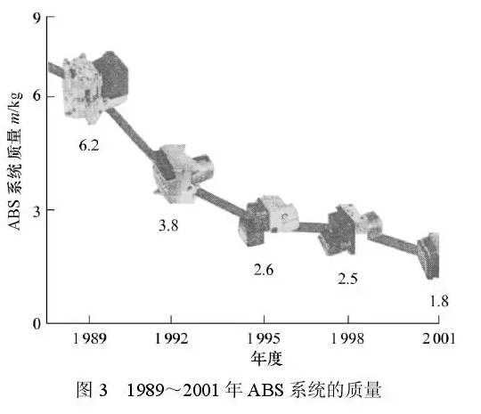
(2) The pursuit of product miniaturization. Along with the improvement in machining accuracy, the size of engineering components is reduced. Figure 3 depicts the quality changes of the ABS system on the vehicle during each period. From 1989 to 2001, it was reduced from 6.2 kg to 1.8 kg. The high integration of electronic circuits requires lowering the surface roughness of silicon wafers, improving the precision of lenses for circuit exposure, and the motion accuracy of semiconductor manufacturing equipment. The miniaturization of components means that the ratio of surface area to volume is increasing, and the surface quality and integrity of the workpiece is becoming more and more important.
(3) The pursuit of high reliability of products. For parts such as bearings that are subjected to relative movement while being loaded, reducing the surface roughness can improve the wear resistance of the parts, improve their working stability, and extend the service life. At present, the surface roughness of Si3N4 ceramic balls used in high-speed high-precision bearings is required to reach several nanometers. The chemically affected layer of the processing metamorphic layer is active and susceptible to corrosion. Therefore, from the viewpoint of improving the corrosion resistance of the part, the metamorphic layer produced by the processing is required to be as small as possible.
(4) The pursuit of high performance products. The improvement of the motion accuracy of the mechanism is beneficial to slow the fluctuation of mechanical properties, reduce vibration and noise. For machines requiring high sealing such as internal combustion engines, good surface roughness reduces leakage and reduces losses. After the Second World War, the aerospace industry required some parts to work in a high temperature environment. Therefore, the use of difficult-to-machine materials such as titanium alloys and ceramics has raised new issues for ultra-precision machining.
The above four aspects are interrelated and jointly promote the development of ultra-precision processing technology. The internationally renowned ultra-precision processing research units and enterprises mainly include LLL Laboratory and Moore Company of the United States, Granfield and Tayler of the United Kingdom, Zeiss and Kugler of Germany, Toshiba Machine of Japan, Toyota Machine and Fujitsu Company. China began to study ultra-precision machining technology in the early 1980s. The main research units include Beijing Machine Tool Research Institute, Tsinghua University, Harbin Institute of Technology, Changchun Institute of Optics and Fine Mechanics, Chinese Academy of Sciences, Dalian University of Technology and Zhejiang University of Technology. Wait.
2 Ultra-precision machining materials
In order to meet the quality requirements of high precision, high reliability, high stability, many metals and their alloys, ceramic materials, optical glass, etc. need to be ultra-precision processed to achieve specific shape, precision and surface integrity. Here we introduce the advanced ceramic materials.
Advanced ceramic materials have become one of the foundations for the development of high-precision machinery, aerospace, military, and optoelectronic information. Advanced ceramics can be roughly classified into functional ceramics and structural ceramics depending on their performance and application range. Functional ceramics mainly refer to ceramics that utilize the direct or coupled effects of electrical, optical, magnetic, chemical or biological aspects of materials to achieve specific functions. They are widely used in electronics, communications, computer, laser and aerospace technologies. Structural ceramic materials have excellent high temperature and wear resistance, and have shown broad application prospects as new materials for high performance mechanical structural parts. Table 1 lists some typical advanced ceramic materials and their uses.
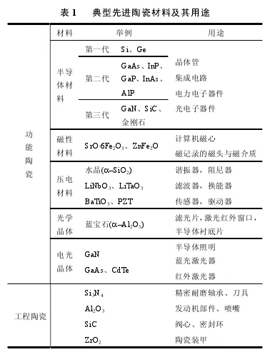
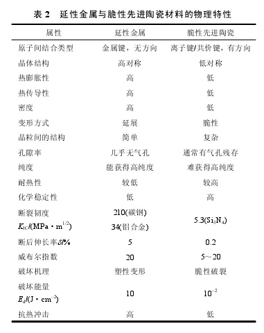
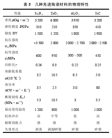
Table 2 shows some of the physical properties of ductile metal materials and brittle advanced ceramic materials. Table 3 shows the physical properties of several advanced ceramic materials. Most advanced ceramic materials are covalent ion bond compounds, with low crystal structure symmetry and few dislocations, resulting in high hardness and brittleness. Silicon nitride, silicon carbide and sapphire are second only to diamond and CBN, and are recognized as typical hard and brittle materials. The difference in physical properties between advanced ceramic materials and metal materials determines the difference in the removal mechanism of the two materials. Advanced ceramic materials are prone to cracks and other surface and subsurface damage during processing, which adversely affect the device's performance and working life.
3, ultra-precision processing technology
3.1 ultra-precision cutting
Ultra-precision cutting begins with SPDT technology, which is supported by air bearing spindles, pneumatic slides, high rigidity, high precision tools, feedback control and ambient temperature control for nanometer surface roughness. The tool used is a large piece of diamond single crystal with a very small cutting edge radius (approximately 20 nm). First used for the processing of copper planar and aspheric optical components. Subsequently, the processing materials were extended to plexiglass, plastic products (such as plastic lenses for cameras, contact lens lenses, etc.), ceramics and composite materials. Ultra-precision cutting technology has also expanded from single-point diamond cutting to multi-point diamond milling.
Because diamond tools cause severe wear when cutting steel, some studies have tried to improve this problem using single crystal CBN, ultra-fine grain hard metal, ceramic tools, but the research results have not yet reached the stage of commercialization. The future trend is to use coating technology to improve the wear of diamond tools in the process of hardening steel. In addition, the processing of tiny parts such as MEMS components requires small tools. Currently, the size of small tools can reach 50-100 μm. However, if the machining geometry is sub-micron or even nano-scale, the tool diameter must be reduced. The trend is to use nanomaterials such as carbon nanotubes to make turning tools or milling cutters with ultra-small tool diameters. In summary, the issue of tool materials and micro-tools will be an important research topic in the future of ultra-precision machining.
3.2 Ultra-precision grinding
In the early stage of ultra-precision machining, the grinding method was neglected because the randomness of the radial cutting edge height and the irregularity of the wear in the grinding wheel limit the improvement of the grinding precision. With the development of superabrasive grinding wheel and grinding wheel dressing technology, ultra-precision grinding technology has gradually formed and developed rapidly.
(1) Super abrasive abrasive wheel. Superabrasive grinding wheels are grinding wheels made of diamond or CBN abrasives. Diamond grinding wheel is suitable for grinding hard and brittle non-ferrous metals and hard alloys, optical glass, ceramics, gemstones and other high-hardness, high-brittle non-metallic materials. CBN grinding wheels are suitable for grinding hardened steel, heat-resistant alloys and high hardness. The high toughness of the metal material, which complements each other, covers almost all of the material being processed. The types and characteristics of superabrasive grinding wheels are shown in Table 4.

The metal bond super-abrasive grinding wheel has high hardness, high strength, strong shape retention ability and good wear resistance, and is often used for precision and ultra-precision grinding and forming grinding. The outstanding problem encountered in the actual use of the multi-layer metal bond super-hard grinding wheel is that the abrasive holding power is low and easy to fall off; the abrasive grain is difficult to be bladed, and the exposedness after the blade is difficult to maintain; the abrasive distribution is random. In view of the problem that the abrasive grain holding power is weak, the active metal is plated on the surface of the abrasive grain, and the chemical reaction and diffusion of the active metal with the abrasive and the binder enhance the holding force of the bonding agent on the abrasive, so that the ruthenium-plated grinding wheel is born. In order to solve the problem that the abrasive grains are difficult to form, the porous structure is introduced into the embryo body to produce a porous metal bond grinding wheel. Electroplating and high-temperature brazing wheels have improved in all three respects. These new superabrasive grinding wheels were all introduced in the 1990s.
Although the above research progress has been made in the production of superabrasive grinding wheels, the active elements in the ruthenium-plated grinding wheel are mainly combined with the abrasive grains by a pure solid or semi-solid reaction, and the bonding strength cannot be compared with the high-temperature strontium grinding wheel. However, the single-layer abrasive of the high-temperature tantalum grinding wheel is no longer supplemented by the subsequent abrasive, although its service life is close to that of the multi-layer abrasive, but it is limited. Although the porous metal bond diamond grinding wheel has the characteristics of easy to trim ceramic-bonded super-abrasive grinding wheel, it is at the expense of bonding strength. To this end, Xu Hongjun and other proposals put forward the idea of developing multi-layered brazing super-abrasive grinding wheels, which combines the high holding power of abrasive grains, the preferential arrangement of abrasive grains and pores, and the high degree of dew of abrasive grains.
(2) Superhard abrasive wheel dressing technology.
The super-hard abrasive wheel has excellent wear resistance and does not require frequent dressing, but it is difficult to trim after initial installation and use of blunt. The traditional dressing method often removes the abrasive grains by shearing and pressing to achieve the purpose of dressing, the dressing process is difficult to control, the dressing precision is low, and the grinding wheel loss is large. To this end, domestic and foreign scholars have also proposed a variety of dressing methods, such as Electro in-process dressing (ELID), Electrochemical in-process controlled dressing (ECD), dry ECD, contact Electro-contact discharge dressing (ECDD), electro-chemical dis-charge machining (ECDM), laser-assisted truing and dressing, water-jet in- Process dressing), ultrasonic dressing, and the like. Among them, ELID technology is the most typical and the application is the most mature. The technology was proposed in 1990 by Dr. Omori Mori of the Institute of Physical Chemistry of Japan and Professor Nakagawa of the University of Tokyo. The basic principle of ELID grinding is the in-line fine dressing of the metal bond grinding wheel by electrolysis during the grinding process, so that the abrasive grain is always processed under the condition of sharp micro edge. The number of micro-blades is large and has the same height, and the grinding marks are fine, so that extremely high machining accuracy is obtained while maintaining high efficiency. They processed silicon wafers with a 4 μm diamond wheel to obtain Rmax 48 nm, Ra4 nm surfaces. The surface of Rmax 8.92 nm and Ra 1.21 nm was obtained by submicron particle size diamond grinding wheel. In 1995, Omori and Chuan Weixiong conducted further research on ELID. The single crystal silicon was polished by ELID with #3 000 000 cast iron-based diamond grinding wheel. The surface roughness after processing reached Rmax 2.34 nm and Ra 0.329 nm.
Scholars from various countries have studied ELID processing of various materials such as Al2O3, Si3N4, Zr O2, SiC, Mn-Zn ferrite, single crystal silicon, optical glass and cermet, including removal mechanism, grinding force and grinding heat. Basic rules such as surface quality, as well as key technologies such as grinding performance of grinding wheels, wheel wear and dressing processes, and developed into a variety of products for many industrial sectors. However, ultra-precision grinding removes the material by forced cutting of the abrasive grains, inevitably leaving a process damage layer on the machined surface. Dasen and Chuan Weixiong processed the silicon wafer and glass with a 40000# diamond wheel to obtain a surface roughness of Ra2.8 nm, but with a surface damage layer of about 1 μm. Liu Shimin et al. studied the thickness and structure of the surface metamorphic layer of two kinds of single crystal silicon wafer grinding samples made by ELID grinding technology by using the scanning electron microscope's selected area electronic channel pattern technology. It was found that the surface roughness of the two single crystal silicon wafer samples was rough. The degrees are 9.5 nm and 22.5 nm, and the thickness of the metamorphic layer is 2.8 μm and 4.8 μm, respectively. In addition, ultra-precision grinding requires high precision and rigidity of the machine. High-speed rotation of the grinding wheel shaft must use expensive bearings, and some degree of vibration is always unavoidable. During the grinding process, the grinding wheel needs to be continuously trimmed to keep the sharpness of the abrasive grains, prevent the grinding debris from clogging the surface of the grinding wheel, and the space of the chip and its retention become the main problem of making the ultrafine abrasive wheel; in addition, grinding In the process, the workpiece and the grinding wheel are mainly in line contact mode, and the processing has a unidirectional property, and it is difficult to ensure the uniformity of the processing surface; the non-magnetic magnetic workpiece is difficult to clamp. These problems limit the surface quality that can be obtained by grinding.
(3) Honing. In the 1980s, flat honing (or fine grinding) was used, which used a grinding-like motion method with a grinding wheel speed of 1/30 to 1/60 of the speed of a conventional grinding wheel. Due to the use of surface contact, the number of abrasive particles involved in grinding increases, the vertical load of each abrasive grain is only 1/50 to 1/100 of the grinding condition, and the heat per unit time of a single average cutting edge is conventional. Grinding is about 1/1 500 to 1/3 000, and the resulting thermal metamorphic layer is small. Due to the small depth of the abrasive grain, the resulting deteriorated layer and residual stress are also small. In addition, in the plane honing process, a batch of workpieces can be processed at the same time; the direction of the cutting force acting on the abrasive grains often changes, so that the probability of breakage of the abrasive grains increases, and the self-twisting effect is remarkable. Therefore, from the point of obtaining surface roughness superior to the grinding process, it has higher efficiency than grinding, and the accuracy of the machine tool is not high. The use of flat honing technology to process advanced ceramic materials has now partially replaced grinding. High-speed grinding of flat fixed abrasives using diamond pellets is based on this principle and has been widely used in the planar processing of ceramics, glass, metals and other materials. However, the use of abrasive grains to force the surface of the workpiece to be finished is limited, and the surface quality that can be obtained is limited.
3.3 Ultra-precision grinding and polishing
Grinding and polishing are the oldest processing methods, and they have always been the most important processing methods for ultra-precision machining. Usually, the grinding is a sub-finishing process, and the flatness is reduced to a few micrometers or less, and the damaged layer produced by the preceding process (usually grinding) is removed. Polishing is currently the main final processing method, the purpose is to reduce the surface roughness and remove the damaged layer formed by grinding to obtain a smooth, damage-free processing surface. The amount of material removed during polishing is very small, about 5 μm. So far, many scholars have proposed a variety of polishing methods, among which the most widely used, the most mature technology is chemical mechanical polishing (CMP) technology.
CMP was developed by IBM in the mid-1980s, first for the production of 64-bit RAM and then for the entire semiconductor industry. YASUNAGA et al. polished sapphire with Si O2, polished single crystal silicon with BaCO3, CeO2 and CaCO3, polished quartz with Fe2O3 and MgO, and obtained a smooth and damage-free surface (surface roughness close to 1 nm). The chemical mechanical polishing was first proposed and verified. the concept of. CMP processing realizes the micro-removal of the workpiece material through the mechanical and chemical interaction between the abrasive-work-machining environment, and can obtain the ultra-smooth, less/no damage processing surface; the processing trajectory is multi-directional, which is beneficial to the surface processing. Uniform consistency; the process follows the "evolution" principle and does not require high precision processing equipment. Because CMP technology can provide the full planarization required for VLSI manufacturing (which is unmatched by other technologies), it has become one of the leading technologies in the semiconductor industry and is expanding its application fields.
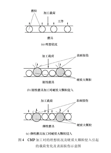
Although CMP technology is considered to be an effective method for obtaining an ultra-smooth, damage-free surface, a surface roughness of 0.1 nm and a very small surface damage layer can be obtained. (In 2000, OGITA used SC1 to clean the silicon wafer on the CMP and found the thickness of the surface damage layer. It is 21 nm), but it also has certain limitations, mainly reflected in the processing accuracy is sensitive to the difference in abrasive grain size. Under ideal conditions, the abrasive grain size between the workpiece and the tool is uniform and the load on the abrasive particles is equal (Figure 4a). When there are hard large particles in the processing zone (abrasive agglomeration or workpiece grinding debris) or entering (large particle dust in the external environment), if the grinding tool is rigid, the processing load is borne by a small amount of large particles, resulting in large particles. The depth of cut of the workpiece is increased to cause damage such as scratches and pits, or large particles are broken under load, but damage is often formed on the surface of the workpiece before crushing (Fig. 4b); for this reason, an elastic polishing pad is usually used ( Asphalt, polyurethane and other materials) to alleviate the negative effects of large particles on the surface of the workpiece, but due to the increased elastic deformation of the position where the polishing pad is in contact with the large particles, the pressure on the large particles increases, which still causes the surface of the workpiece to be scratched. Traces and other forms of damage (Figure 4c). At present, it is only possible to avoid the damage of the hard large particles to the processing surface by improving the purification degree of the processing environment and the consistency of the abrasive grain size, but it is expensive and cannot completely avoid the invasion of large particles. Surface scratches caused by hard large particles cause a large number of workpieces to be repaired or scrapped, which seriously hinders the improvement of overall processing efficiency. How to effectively avoid damage caused by hard large particles has become an urgent problem to be solved in the polishing process. In addition, the material removal is mainly based on the three-body wear mechanism. The abrasive particles mainly remove the material in a rolling manner. The amount of abrasive particles involved in material removal per unit time is small, the material removal rate is low, and the chemical composition and the abrasive particles are harmful. Environment and high processing costs.
In addition to CMP technology, the classic ultra-precision grinding and polishing methods are as follows.
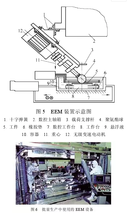
(1) Elastic emission machine (EEM). Osaka University of Japan TSUWA et al. studied the feasibility of removing materials at the atomic level on the surface of the workpiece, and established the theory of elastic emission processing. The processing principle and production equipment are shown in Figures 5 and 6, respectively. The EEM technology uses the immersion working mode to drive the abrasive with a particle size of several tens of nanometers in the polishing liquid by using a polyurethane ball rotating at a high speed on the surface of the workpiece, and impact the surface of the workpiece with the incident angle as small as possible, through the chemistry between the abrasive particles and the workpiece. The function of removing the workpiece material, the surface layer of the workpiece is not plastically deformed, and no defects such as lattice transposition are generated, which is extremely advantageous for processing functional crystal materials. TSUWA uses a polyurethane ball as a tool to elastically eject single crystal silicon with Zr O2 micropowder with a surface roughness of 0.5 nm.
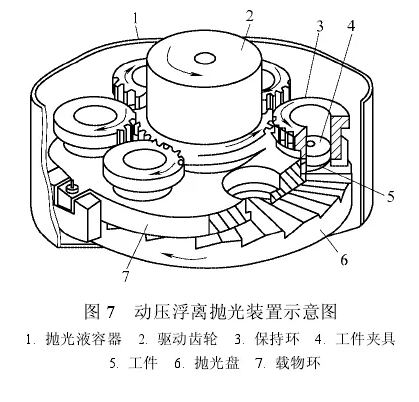
(2) Dynamic pressure floating polishing. WATANABE et al. developed a dynamic pressure float polishing technique using the principle of dynamic pressure bearings, as shown in Figure 7. By making a plurality of inclined planes along the circumferential direction of the polishing disc, the workpiece is floated on the surface of the polishing disc by the hydraulic pressure generated when the polishing disc is rotated, and the workpiece is polished by the polishing particles in the floating gap. Since there is no frictional heat and abrasive wear, the standard surface does not change, so the precise workpiece surface can be obtained repeatedly. Using this polishing method to process a silicon wafer with a diameter of 75 mm, a flatness of 0.3 μm and a surface roughness of 1 nm are obtained.
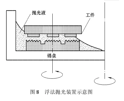
(3) Float polishing. In 1977, researchers such as NAMBA in Japan proposed a float polishing process for processing polished head materials. The principle is shown in Figure 8. The process uses a highly flat plane with a tin-polished disc with concentric circles or spiral grooves, which covers the entire surface of the polishing disc, allowing the polishing disc and the workpiece to rotate at high speed, and the polishing fluid is dynamically pressed between the two. The liquid state forms a liquid film, and the abrasive in the liquid film impacts the surface of the workpiece at a high speed to remove the material. NAMBA and other SiO2 colloidal, CeO2 and Al2O3 polisher sapphire (001) surfaces were float polished with a surface roughness of less than 1 nm. Compared with other polishing methods, the polished workpiece edge geometry is regular, the sub-surface layer is not damaged, the surface residual stress caused by polishing is extremely small, and the crystal surface has a perfect crystal lattice. Float polishing is similar to EEM polishing, except that the float polishing uses a hard tin plate as the grinding tool, while the EEM method uses a polyurethane rubber wheel as the grinding tool.
(4) Low temperature polishing. Low-temperature polishing refers to polishing with a polishing liquid that has condensed into a solid state in a low-temperature environment. Han Rongjiu etc. freezes the colloidal SiO2 into a solid film and then maintains the temperature between –50 and –30 °C. The K9 glass is processed to obtain a surface roughness of Ra 0.4 nm. WU et al. combined the low-temperature polishing method with the non-abrasive polishing technology, and proposed a non-abrasive low-temperature polishing method, that is, solid ice with deionized water at a low temperature as a polishing tool. MaQ glass can be processed to obtain a surface roughness of Ra0.48 nm (the surface roughness of the workpiece before processing is Ra1.3 nm). Analysis of the water produced after processing, no solid glass fragments were found, and the material was judged to be removed by hydrolysis, thereby effectively preventing the occurrence of defects such as micro-scratches. After polishing for 40 h, the mass change of the workpiece was not measured with an electronic balance with an accuracy of 0.01 g. However, due to the extremely high cost of maintaining a low temperature, vacuum environment, applications are limited.
(5) Magnetic field assisted polishing. Magnetic field assisted polishing mainly includes magnetic abrasive finishing (MAF), magnetic floating polishing (MPF) and magnetorheological finishing (MRF).
The concept of magnetic grinding was first proposed by former Soviet engineer Kagolow in 1938. During processing, the magnetic abrasive particles (microparticles that must have both magnetizable and abrasive properties) form a "magnetic brush" under the action of a magnetic field, and the "magnetic brush" and the workpiece are generated by the relative movement of the magnetic pole and the workpiece. Interference with friction to complete processing. The processing pressure can be controlled by a magnetic field. FOX et al. used a 0.1 μm diamond micropowder to magnetically grind the stainless steel roller to obtain a Ra10 nm surface. The magnetic abrasive grain processing has almost no restrictions on the geometric shape of the workpiece, and the precision of the equipment is not high. In particular, the abrasive grain is not in rigid contact with the surface of the workpiece, so even if there are a few large abrasive grains or the surface of the workpiece occasionally appears unevenly hard. At the point, the surface of the workpiece is not scratched due to a sudden change in the cutting resistance. However, in the MAF research papers published in the past, almost 90% of the experiments were made of sintered magnetic abrasives because of the complicated sintering process, high cost and limited application.
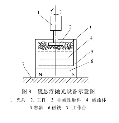
Magnetic floating polishing was developed by TANI et al., and has been continuously developed by many scholars such as UMEHARA, CHILDS, and KATO. The device is shown in Figure 9. When the non-magnetic abrasive is mixed into the magnetic fluid and placed in a magnetic field, the magnetic fluid is attracted to the side of the high magnetic field due to the action of the ferromagnetic particles in the magnetic fluid, and the non-magnetic abrasive grains are pushed to the opposite direction of the movement of the magnetic fluid. The abrasive particles on one side of the magnetic field are pressed against the rotating workpiece by the buoyancy of the magnetic fluid for polishing. JIANG et al. used the magnetic floating polishing method to process Si3N4 ceramic balls (Ce O2, 5 μm), and obtained the surface precision of Ra 4 nm and Rz 40 nm.
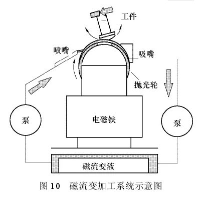
Magnetorheological processing was proposed by KORDONSKY et al. in the early 1990s. They combine electromagnetism and fluid dynamics theory, using magnetorheological fluids (suspensions consisting of magnetic particles, base fluids, and stabilizers) in the magnetic field. The rheological properties in the polishing of the optical glass. The rheological properties of the magnetorheological fluid can be controlled by the adjustment of the applied magnetic field strength. The magnetorheological processing device is shown in Figure 10. The magnetorheological fluid is sprayed by a nozzle on a rotating polishing wheel, and the magnetic pole is placed under the polishing wheel to form a high gradient magnetic field near the narrow gap formed by the workpiece and the polishing wheel. When the magnetorheological fluid on the polishing wheel is transferred to the vicinity of the small gap formed by the workpiece and the polishing wheel, the high gradient magnetic field causes it to coagulate and harden, becoming a viscoplastic Bingham medium. When a Bingham medium having a high moving speed passes through a small gap, a large shear force is generated in a region where the surface of the workpiece comes into contact with it, so that the surface material of the workpiece is removed. During the polishing process, selective removal of the surface of the workpiece can be achieved by controlling the sweep rate (or residence time) of the magnetorheological fluid in the workpiece. 1997 年 JACOBS 等对红外材料 BK7、CaF2、LiF 等进行磁流变抛光,获得表面粗糙度小于 5 nm的光滑表面。 2006 年孙希威等用磁流变抛光加工了R41.3 mm、口径 20 mm 的 K9 光学玻璃球面工件,获得了表面粗糙度 8.441 nm、面形精度57.911 nm PV 的表面。
(6) 气囊式抛光。气囊式抛光技术是 2000 年伦敦学院大学光学科学实验室和 Zeeko 有限公司联合提出的。抛光工具外面包有磨料薄膜层(如聚氨酯抛光垫、抛光布等)的胶皮气囊。抛光工作时,工具气囊旋转形成抛光运动,工件对气囊抛光工具作相对的进给运动,使工件的全部表面都被能抛光加工。工具气囊同时还作摆动(摆动中心为气囊曲面的曲率中心),使磨料薄膜层均匀磨损。由于工具气囊具有弹性,可以自动适应工件的曲面形状,故同一工具可用于抛光不同外形的曲面。该方法适于大型自由曲面的超精密加工。
(7) 应力盘抛光。为实现大型非球面元件的超精密加工,诞生了应力盘抛光方法。该方法采用大尺寸刚性盘作为基盘,在周边可变应力的作用下,盘的面形可以实时地变形成所需要的面形,以适配非球面的不同位置上的吻合研磨。应力盘抛光技术具有优先去除表面最高点或部位的特点,具有平滑中高频差的趋势,可以很好地控制中高频差的出现、有效地提高加工效率。2002 年 MARTIN 等用应力盘抛光技术对 Magellan 望远镜 6.5 mf/1.25 主镜和Large Binocular 望远镜 8.4 mf/1.14 主镜进行了抛光,这些大型镜片都是非球面镜,加工后形状误差为0.01%,表面粗糙度为 20 nm。
(8) 电解抛光。电解抛光又称电化学抛光,起源于 20 世纪初。1930 年法国电话公司Jacquet 首次提出电解抛光技术,并进行了系统研究。目前,解释电解抛光过程比较合理的理论是薄膜理论。薄膜理论认为,电解抛光时,靠近金属试样阳极表面的电解液,在试样上随着表面凹凸高低不平形成一层薄厚不均匀的粘性薄膜。由于电解液搅拌流动,在靠近试样表面凹陷的地方,扩散流动得较慢,因而形成的膜较厚,而在凸起的地方薄膜较薄。由于试样表面各处的电流密度相差很多,凸起顶峰地方电流密度很大,金属快速地溶解于电解液中,而凹陷部分金属则溶解慢,结果使得粗糙的表面变得平整从而达到抛光的目的。2003 年 HUANG 等对高速钢进行电解抛光,获得 Ra30~50 nm 的表面。
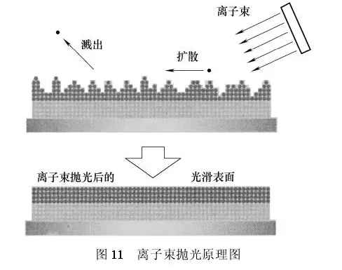
(9) 离子束抛光。离子束抛光是把中性离子在电场中加速,撞击工件表面的原子或分子,使其逸出表面从而将材料去除(图 11)。由于被加工材料以原子或分子为单位去除,可获得纳米级高质量加工表面。LI等用氟离子束对 CMP 后的 50 mmGaSb外延片进行超精加工,使其表面粗糙度由 0.7 nm 降低到 0.18 nm。离子束抛光可加工的材料范围较广,对工件尺寸没有严格控制,并且可加工球面、非球面和非对称面形。
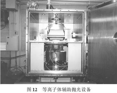
(10) 等 离 子 体 辅 助 抛 光 (Plasma-assisted chemical ething,PACE)。等离子体辅助抛光又称化学 蒸 发 加 工 (chemical vaporization machining ,CVM),是在真空环境下进行,其设备如图 12 所示。将化学气体(通常为卤素类气体,如 CF、Cl2等)激发成活性等离子体,与加工面产生化学反应,生成挥发性物质从而达到材料去除的目的。这种加工方法实用化的一种就是等离子腐蚀。
PACE加工具有抛光效率高,工作不受机械压力,没有机械变形,加工表面无亚表面损伤、无污染,加工球面和非球面难易相当等优点。目前Perkin-Elmer 公司用该技术已在φ 0.5 m~1.0 m 的非球面上加工出面形精度小于 1/50λ,表面粗糙度小于 0.5 nm 的表面。
(11) 激光抛光。激光抛光技术是利用激光与材料表面相互作用进行加工,它遵循激光与材料作用的普遍规律。激光与材料间的作用方式有热作用和光化学作用,可把激光抛光分为热抛光和冷抛光。热抛光是利用激光的热效应,通过熔化、蒸发等过程去除材料。因此只要材料的热物理性能好,都可以用它来进行抛光,但由于温度梯度大而产生的热应力大,易产生裂纹,因此热抛光的效果不是很好。冷抛光是利用材料吸收光子后,表层材料的化学键被打断或者是晶格结构被破坏,从而实现材料的去除。利用光化学作用时,热效应可以被忽略,因此热应力很小,不产生裂纹,也不影响周围材料,且容易控制材料的去除量,特别适合于硬脆性材料的精密加工UDREA 等利用 CO2激光器对光纤的端面进行抛光,得到的 Ra 100 nm 表面粗糙度。激光抛光是一种非接触抛光,不仅能对平面进行抛光,还能对各种曲面进行抛光。而且对环境的污染小,可以实现局部抛光,特别适用于超硬材料和脆性材料的精抛,具有良好的发展前景。但目前激光抛光作为一种新技术还处于发展阶段,还存在着设备和加工成本高、加工过程中的检测技术和精度控制技术要求比较高等缺点。
4、几类超精密加工技术的比较及半固
着磨粒加工 超精密加工的精度不仅随时代变化,即使在同一时期,工件的尺寸、形状、材质、用途和加工难度不同,超精密加工的精度也不同。对上述几种典型的超精密加工技术可进行定性比较,如表 5 所示。
如前所述,超精密切削以高刚度、高精度的设备为支撑,可获得纳米级表面粗糙度,具有较高的材料去除率。但同一时间仅能加工一件工件,故而生产效率可能不及多片加工的磨削或研磨抛光技术。同样超精密砂轮磨削也要求高刚度、高精度的设备,材料去除率高,使用超细磨粒砂轮甚至可以获得埃级表面粗糙度。但超细磨粒砂轮的制备及其容屑空间的保持等问题尚未成熟。由砂轮磨削发展而来的平面珩磨技术采用降低砂轮转速的方法,减少磨削加工的表面损伤,利用工件与砂轮的面接触形式可以补偿因转速降低带来的磨削效率的损失。对设备精度要求不高,但与超精密切削、磨削一样,通过被加工材料的强制性去除方式完成加工,限制了所能获得的表面质量,不可避免地在加工表面留下加工损伤层。相对于超精密磨削、珩磨等固着磨粒加工,利用游离磨粒进行加工的超精密研磨抛光技术,如 CMP、EEM 等,可获得更高的表面质量和更小的加工损伤层。但由于加工过程中磨粒处于游离状态,磨粒对工件的作用是非强制性的,材料去除率更低。且加工精度和加工效率对磨粒尺寸差异十分敏感,硬质大颗粒的侵入可导致大量工件返修或报废,在降低加工精度和加工效率同时引起生产成本的大幅上升。磁性磨粒加工虽然降低了对硬质大颗粒的敏感度,但磁性磨粒复杂而昂贵的制备过程限制其发展和应用。离子束抛光等不使用磨粒的超精密抛光方法,以原子为单位去除材料,可获得极高的表面粗糙度,但材料去除率极低,通常仅用于 CMP 等抛光工艺后,使工件表面质量和损伤层进一步提高。此类技术通常需要特殊的设备,要求高精度的检测技术和控制技术,加工成本高。
为实现高效精密加工,诞生了将固着磨粒加工和游离磨粒加工进行整合的半固着磨粒加工概念。SHIMADA 等提出了一种使用半固态的磁性抛光体(Magnetic compound fluid polishing tool,MPT)进行超精密加工的方法。该方法将磁性复合流体(Magnetic compound fluid,MCF)和磨粒、植物纤维均匀混合后在磁场条件下压缩制得 MPT,MPT 在磁场作用下为半固态,以此对工件进行加工。他们使用微米级铁粉构成的 MPT 对 SUS430 不锈钢进行抛光,获得 Ra15 nm 的表面。目前此方面研究尚处于起步阶段。
针对大批量生产的氮化硅陶瓷、蓝宝石单晶等硬脆难加工先进陶瓷材料超光滑无损伤表面高效加工的要求,作者提出一种半固着磨粒加工技术。磨具中的磨粒处于半固着状态,磨具表层对硬质大颗粒具有“陷阱”效应,即硬质大颗粒侵入时,可使之陷入磨具表面,从而主动防止或降低大颗粒对加工表面造成的损伤。同时,该技术具有比研磨更高的加工效率,表面加工质量甚至可以达到抛光的水平。
5、超精密加工的发展趋势
(1) 高精度、高效率。高精度与高效率是超精密加工永恒的主题。总的来说,固着磨粒加工不断追求着游离磨粒的加工精度,而游离磨粒加工不断追求的是固着磨粒加工的效率。当前超精密加技术如 CMP、EEM 等虽能获得极高的表面质量和表面完整性,但以牺牲加工效率为保证。超精密切削、磨削技术虽然加工效率高,但无法获得如 CMP、EEM 的加工精度。探索能兼顾效率与精度的加工方法,成为超精密加工领域研究人员的目标。半固着磨粒加工方法的出现即体现了这一趋势。另一方面表现为电解磁力研磨、磁流变磨料流加工等复合加工方法的诞生。
(2) 工艺整合化。当今企业间的竞争趋于白热化,高生产效率越来越成为企业赖以生存的条件。在这样的背景下,出现了“以磨代研”甚至“以磨代抛”的呼声。另一方面,使用一台设备完成多种加工(如车削、钻削、铣削、磨削、光整)的趋势越来越明显。
(3) 大型化、微型化。为加工航空、航天、宇航等领域需要的大型光电子器件(如大型天体望远镜上的反射镜),需要建立大型超精密加工设备。为加工微型电子机械、光电信息等领域需要的微型器件(如微型传感器、微型驱动元件等),需要微型超精密加工设备(但这并不是说加工微小型工件一定需要微小型加工设备)。
(4) 在线检测。尽管现在超精密加工方法多种多样,但都尚未发展成熟。例如,虽然 CMP 等加工方法已成功应用于工业生产,但其加工机理尚未明确。主要原因之一是超精密加工检测技术还不完善,特别是在线检测技术。从实际生产角度讲,开发加工精度在线测量技术是保证产品质量和提高生产率的重要手段。
(5) 智能化。超精密加工中的工艺过程控制策略与控制方法也是目前的研究热点之一。以智能化设备降低加工结果对人工经验的依赖性一直是制造领域追求的目标。加工设备的智能化程度直接关系到加工的稳定性与加工效率,这一点在超精密加工中体现更为明显。目前,即使是台湾的部分半导体工厂,生产过程中关键的操作依然由工人在现场手工完成。
(6) 绿色化。磨料加工是超精密加工的主要手段,磨料本身的制造、磨料在加工中的消耗、加工中造成的能源及材料的消耗、以及加工中大量使用的加工液等对环境造成了极大的负担。我国是磨料、磨具产量及消耗的第一大国,大幅提高磨削加工的绿色化程度已成为当务之急发达国家以及我国的台湾地区均对半导体生产厂家的废液、废气排量及标准实施严格管制,为此,各国研究人员对CMP 加工产生的废液、废气回收处理展开了研究。绿色化的超精密加工技术在降低环境负担的同时,提高了自身的生命力。
6、结论
出于对产品高质量、小型化、高可靠性和高性能的追求,超精密加工技术得以迅速发展,现已成为现代制造工业的重要组成部分,其加工的对象已从军用品拓展到民用品,并以后者为重心。超精密加工技术的发展推动了国防、航空航天、光电信息等高科技产业的发展,同时也极大地改变了人类的生活方式、改善了人们的生活水平。超精密加工技术正迎来一个繁荣的时代。鉴于军事、信息等产业对高精度先进陶瓷元件的巨大需求,新的高性能先进陶瓷材料不断涌现,这类材料的超精密加工成为经久不衰的研究热点。超精密切削、超精密磨削、超精密研磨与抛光技术已取得长足的进展,加工后工件表面精度可达纳米级或亚纳米级,并且加工方法目趋多样化。总的来说,超精密磨削、珩磨等固着磨粒超精密加工技术正在追求游离磨粒加工技术的加工精度,而游离磨粒超精密加工技术正在追求固着磨粒加工的效率。超精密加工技术正向着适于大批量生产的高效高质量、低成本、环境友好的方向发展。
Many 3D printing proponents claim that 3D printing is a good substitute for injection molding that requires a mold. Is it really? Let’s go and see what everyone’s opinions are like. Additive...
Model NO.: HW-386 Runner: Hot Runner Design Software: UG Installation: Fixed Certification: ISO Standard: HASCO Customized: Customized Trademark: HOWE or Custom Transport Package: Exported Wooden...
In order to ensure the safety of the plateau roads, the research and development work of the plateau new passenger cars initiated by the Ministry of Transport of the People's Republic of China to...
Model NO.: CKNC6180 Performance Classification: Economical CNC Machine Tools Certification: CE, ISO 9001 Condition: New Max.Swing Over Bed: 800mm Max. Swing Over Slide: 480 Max. Processing Lathe:...
Email to this supplier

ABOUT
PRODUCTS
Links
Follow Us

Privacy statement: Your privacy is very important to Us. Our company promises not to disclose your personal information to any external company with out your explicit permission.

Fill in more information so that we can get in touch with you faster
Privacy statement: Your privacy is very important to Us. Our company promises not to disclose your personal information to any external company with out your explicit permission.